Supermicro X9DBS-F Bedienungsanleitung
Supermicro
Hauptplatine
X9DBS-F
Lesen Sie kostenlos die 📖 deutsche Bedienungsanleitung für Supermicro X9DBS-F (99 Seiten) in der Kategorie Hauptplatine. Dieser Bedienungsanleitung war für 11 Personen hilfreich und wurde von 2 Benutzern mit durchschnittlich 4.5 Sternen bewertet
Seite 1/99

USER’S MANUAL
Revision 1.0a
X9DBS-F
X9DBS-F-2U

Manual Revision 1.0a
Release Date: October 31, 2013
Unless you request and receive written permission from Super Micro Computer, Inc., you may not
copy any part of this document.
Information in this document is subject to change without notice. Other products and companies
referred to herein are trademarks or registered trademarks of their respective companies or mark
holders.
Copyright © 2013 by Super Micro Computer, Inc.
All rights reserved.
Printed in the United States of America
The information in this User’s Manual has been carefully reviewed and is believed to be accurate.
The vendor assumes no responsibility for any inaccuracies that may be contained in this document,
and makes no commitment to update or to keep current the information in this manual, or to notify
any person or organization of the updates. Please Note: For the most up-to-date version of this
manual, please see our Website at www.supermicro.com.
Super Micro Computer, Inc. ("Supermicro") reserves the right to make changes to the product
described in this manual at any time and without notice. This product, including software and docu-
mentation, is the property of Supermicro and/or its licensors, and is supplied only under a license.
Any use or reproduction of this product is not allowed, except as expressly permitted by the terms
of said license.
IN NO EVENT WILL SUPER MICRO COMPUTER, INC. BE LIABLE FOR DIRECT, INDIRECT,
SPECIAL, INCIDENTAL, SPECULATIVE OR CONSEQUENTIAL DAMAGES ARISING FROM THE
USE OR INABILITY TO USE THIS PRODUCT OR DOCUMENTATION, EVEN IF ADVISED OF
THE POSSIBILITY OF SUCH DAMAGES. IN PARTICULAR, SUPER MICRO COMPUTER, INC.
SHALL NOT HAVE LIABILITY FOR ANY HARDWARE, SOFTWARE, OR DATA STORED OR USED
WITH THE PRODUCT, INCLUDING THE COSTS OF REPAIRING, REPLACING, INTEGRATING,
INSTALLING OR RECOVERING SUCH HARDWARE, SOFTWARE, OR DATA.
Any disputes arising between the manufacturer and the customer shall be governed by the laws of
Santa Clara County in the State of California, USA. The State of California, County of Santa Clara
shall be the exclusive venue for the resolution of any such disputes. Supermicro's total liability for
all claims will not exceed the price paid for the hardware product.
FCC Statement: This equipment has been tested and found to comply with the limits for a Class
A digital device pursuant to Part 15 of the FCC Rules. These limits are designed to provide
reasonable protection against harmful interference when the equipment is operated in a commercial
environment. This equipment generates, uses, and can radiate radio frequency energy and, if not
installed and used in accordance with the manufacturer’s instruction manual, may cause harmful
interference with radio communications. Operation of this equipment in a residential area is likely
to cause harmful interference, in which case you will be required to correct the interference at your
own expense.
California Best Management Practices Regulations for Perchlorate Materials: This Perchlorate
warning applies only to products containing CR (Manganese Dioxide) Lithium coin cells. “Perchlorate
Material-special handling may apply. See www.dtsc.ca.gov/hazardouswaste/perchlorate”.
WARNING: Handling of lead solder materials used in this
product may expose you to lead, a chemical known to
the State of California to cause birth defects and other
reproductive harm.

Preface
This manua l is w r itten f or sy stem i n tegra tors , P C tech nici ans a nd
knowledgeable PC users. It provides information for the installation and use of the
X9DBS-F/X9DBS-F-2U motherboard.
About This Motherboard
The Super X9DBS-F/X9DBS-F-2U motherboard supports dual Intel E5-2400 (Sock-
et B2) processors and Intel QPI (QuickPath Interface) Technology (V.1.1), providing
point-to-point connections with transfer speeds of up to 8.0 GT/s. With the C602J
chipset built in, the X9DBS-F/X9DBS-F-2U motherboard supports Intel® Manage-
ment Engine (ME), Rapid Storage Technology, Digital Media Interface (DMI), PCI-
E Gen. 3.0, and DDR3 memory of up to 1600 MHz (@ 1.5V), greatly enhancing
system performance. This motherboard is intended to be used in Supermicro SBB
platforms. Please refer to our website at http://www.supermicro.com for processor
and memory update and support.
Manual Organization
Chapter 1 describes the features, specications and performance of the mother-
board. It also provides detailed information on the Intel C602J chipset.
Chapter 2 provides hardware installation instructions. Read this chapter when in-
stalling the processor, memory modules, and other hardware components into the
system. If you encounter any problems, see , which describes troubleChapter 3 -
shooting procedures for video, memory, and system setup stored in the CMOS.
Chapter 4 includes an introduction to the BIOS, and provides detailed information
on running the CMOS Setup utility.
Appendix A provides BIOS Error Beep Codes.
Appendix B lists software installation instructions.
Preface
iii

iv
Conventions Used in the Manual
Pay special attention to the following symbols for proper system installation and to
prevent damage to the system or injury to yourself:
Warning: Important information is given to ensure proper system installation or to avoid
causing damage to the system or causing injury to yourself.
Note: Additional information is given to differentiate among various models
or to provide information for correct system setup.
X9DBS-F/X9DBS-F-2U Motherboard User’s Manual

Preface
v
Contacting Supermicro
Headquarters
Address: Super Micro Computer, Inc.
980 Rock Ave.
San Jose, CA 95131 U.S.A.
Tel: +1 (408) 503-8000
Fax: +1 (408) 503-8008
Email: marketing@supermicro.com (General Information)
support@supermicro.com (Technical Support)
Web Site: www.supermicro.com
Europe
Address: Super Micro Computer B.V.
Het Sterrenbeeld 28, 5215 ML
's-Hertogenbosch, The Netherlands
Tel: +31 (0) 73-6400390
Fax: +31 (0) 73-6416525
Email: sales@supermicro.nl (General Information)
support@supermicro.nl (Technical Support)
rma@supermicro.nl (Customer Support)
Asia-Pacic
Address: Super Micro Computer, Inc.
3F, No. 150, Jian 1st Rd.
Zhonghe Dist., New Taipei City 23511
Taiwan (R.O.C)
Tel: +886-(2) 8226-3990
Fax: +886-(2) 8226-3992
Web Site: www.supermicro.com.tw
Technical Support:
Email: support@supermicro.com.tw
Tel: +886-(2)-8226-3990

vi
Table of Contents
Preface
Chapter 1 Overview
1-1 Overview ......................................................................................................... 1-1
1-2 Processor and Chipset Overview...................................................................1-11
1-3 Special Features ........................................................................................... 1-12
1-4 PC Health Monitoring .................................................................................... 1-12
1-5 ACPI Features ............................................................................................... 1-13
1-6 Power Supply ................................................................................................ 1-13
1-7 Super I/O ....................................................................................................... 1-13
1-8 Advanced Power Management ..................................................................... 1-14
Intel® Intelligent Power Node Manager (IPNM) ............................................ 1-14
Management Engine (ME) ............................................................................ 1-14
1-9 Introduction to the IPMI Controller 1-14 ................................................................
WPCM450R DDR2 Memory Interface .......................................................... 1-15
WPCM450R PCI System Interface ............................................................... 1-15
Other Features Supported by the WPCM BMC Controller ........................... 1-15
1-10 NVDIMM Memory Support ............................................................................ 1-16
Chapter 2 Installation
2-1 Standardized Warning Statements ................................................................. 2-1
2-2 Static-Sensitive Devices .................................................................................. 2-4
2-3 Processor and Heatsink Installation................................................................ 2-5
Installing an LGA 1356 Processor .................................................................. 2-5
Installing a Passive CPU Heatsink ................................................................. 2-7
Removing the Passive Heatsink ..................................................................... 2-8
2-4 Installing and Removing the Memory Modules ............................................... 2-9
Installing & Removing DIMMs ......................................................................... 2-9
Removing Memory Modules ........................................................................... 2-9
2-5 Motherboard Installation ................................................................................ 2-13
Tools Needed ................................................................................................ 2-13
Location of Mounting Holes .......................................................................... 2-13
Installing the Motherboard ............................................................................ 2-14
2-6 Control Panel Connectors and I/O Ports ...................................................... 2-15
Back Panel Connectors and I/O Ports .......................................................... 2-15
Back Panel I/O Port Locations and Denitions ........................................... 2-15
Keyboard/Video/Mouse 2-16 ............................................................................
X9DBS-F/X9DBS-F-2U Motherboard User’s Manual

viii
Appendix A BIOS Error Beep Codes
A-1 BIOS Error Beep Codes .................................................................................A-1
Appendix B Software Installation Instructions
B-1 Installing Software Programs ..........................................................................B-1
B-2 Installing SuperDoctor®5 (Available when a newer version of CPU is installed
onboard) B-2 .....................................................................................................................
X9DBS-F/X9DBS-F-2U Motherboard User’s Manual

Chapter 1: Overview
1-1
Chapter 1
Overview
1-1 Overview
Checklist
Congratulations on purchasing your computer motherboard from an acknowledged
leader in the industry. Supermicro boards are designed with the utmost attention to
detail to provide you with the highest standards in quality and performance.
This motherboard is intended to be used in Supermicro's 2U/3U SBB chassis as
an integrated platform solution. No retail package will be included in the shipment.
Note: For your system to work properly, please follow the links below to
download all necessary drivers/utilities and the user's manual for your
motherboard.
SMCI product manuals: http://www.supermicro.com/support/manuals/
Product Drivers and utilities: ftp://ftp.supermicro.com/
If you have any questions, please contact our support team at support@supermicro.
com.

1-2
X9DBS-F/X9DBS-F-2U Motherboard User’s Manual
Motherboard Image
Note: All graphics shown in this manual were based upon the latest PCB
revision available at the time of publishing of the manual. The motherboard
you've received may or may not look exactly the same as the graphics
shown in this manual.

Chapter 1: Overview
1-3
Motherboard Layout
Note : For the latest CPU/Memory updates, please refer to our website at
http://www.supermicro.com/products/motherboard/ for details.
Fan 6
Fan 5
Fan 4
JPL1
LAN1
LAN2
JKVM1
VGA/USB/COM1
External SAA
D95
Slot1 PCI-E 3.0x24
CPU2 Port1 CPU2 Port3
JPI2C2 JPI2C1
JPLD1
JDBS5
BIOS JBT1 PCH
USB3
I-SATA0
I-SATA1
JSD1
JSD2
JWD1
P2-DIMMD1
P2-DIMME1
P2-DIMMF1
JPME1
JPME2
Fan1
Fan2Fan3
JTPM1
LED2
Battery
LED10
JOH1
M13 M9 M8 M7 M6 M4
M3 M2 M1
LED3
LED11
J21
LED13
LED12
P1-DIMMA1
P1-DIMMB1
P1-DIMMC1
BMC
SAS
Re-Driver
SAS MEZZANINE HEADER
CPU1
CPU2
X9DBS-F
Rev. 1.10
LAN
Intel i350
SAS
Re-Driver
JCAP_PWR1

1-4
X9DBS-F/X9DBS-F-2U Motherboard User’s Manual
Notes:
•See Chapter 2 for detailed information on jumpers, I/O ports and JF1 front
panel connections.
•" " indicates the location of "Pin 1".
•Jumpers/LED Indicators/connectors/headers not indicated or documented are
for testing only.
•Use only the correct type of onboard CMOS battery as specied by the manu-
facturer. Do not install the onboard battery upside down to avoid possible short
circuit.
X9DBS-F/X9DBS-F-2U Jumpers
Fan 6
Fan 5
Fan 4
JPL1
LAN1LAN2
JKVM1
VGA/USB/COM1
External SAA
D95
Slot1 PCI-E 3.0x24
CPU2 Port1 CPU2 Port3
JPI2C2 JPI2C1
JPLD1
JDBS5
BIOS JBT1 PCH
USB3
I-SATA0
I-SATA1
JSD1
JSD2
JWD1
P2-DIMMD1
P2-DIMME1
P2-DIMMF1
JPME1
JPME2
Fan1
Fan2Fan3
JTPM1
LED2
Battery
LED10
JOH1
M13 M9 M8 M7 M6 M4
M3 M2 M1
LED3
LED11
J21
LED13
LED12
P1-DIMMA1
P1-DIMMB1
P1-DIMMC1
BMC
SAS
Re-Driver
SAS MEZZANINE HEADER
CPU1
CPU2
X9DBS-F
Rev. 1.10
LAN
Intel i350
SAS
Re-Driver
JCAP_PWR1

Chapter 1: Overview
1-5
X9DBS-F/X9DBS-F-2U Jumpers
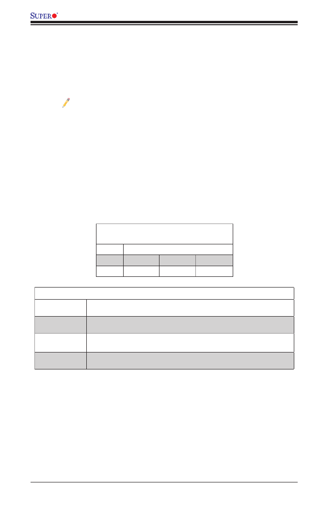
Jumper Description Default Setting
JBT1 Clear CMOS See Chapter 3
JI2C1/JI2C2 SMB to PCI-E Slots Open (Normal)
JPL1 GLAN 1/2 Enable Pins 1-2 (Enabled)
JPME1 ME Firmware Pins 1-2 (Normal)
JPME2 ME Mode (Select) Pins 1-2 (Normal)
JWD1 Watch Dog Pins 1-2 (Reset)
X9DBS-F/X9DBS-F-2U Connectors
Connectors Description
Battery Onboard CMOS Battery (See Chpt. 3 for Used Battery Disposal
Info.)
FAN1-6 CPU/System Fan Headers
J21 SAS Mezzanine Header
JCAP_PWR1 Super-CAP Power Charger Connector
JKVM1 Keyboard/VGA/Mouse Connector
JOH1 Overheat/Fan Fail LED
JSD1/JSD2 SATA DOM (Device On Module) Power Connectors
JTPM1 TPM (Trusted Platform Module)/Port 80
LAN1/LAN2 Gigabit Ethernet LAN Ports 1/2 (LAN1/LAN2)
(External) SAS External Serial-Link SAS Connector (with SAS Mezzanine card)
(I-)SATA 0/1 Intel SATA Connectors 0/1
Slot1 PCI-Exp. 3.0 x24 Slot for 2U/3U Riser Card
USB3 Type A USB Port 3
X9DBS-F/X9DBS-F-2U LED Indicators
LED Description State Status
D95
BMC Heartbeat
System Heartbeat
D95: Up (BMC Heartbeat) Green: BMC Active
D95: Down (System Heartbeat) Green: Sys. Active
LED2 SATA LED Green: Blinking SATA: Active
LED3 Onboard Power Green: On Onboard PWR Connected
LED10/
LED11 SAS Activity LED SAS: ActiveGreen: Blinking

1-6
X9DBS-F/X9DBS-F-2U Motherboard User’s Manual
Motherboard Features
CPU • Dual Intel®
E5-2400 (Socket B2 up to 95W) proces-
sors; each processor supports two full-width Quick-
Path Interconnect (QPI) links of up to 8.0 GT/s per link
and with data transfer rate of up to 16 GB/s direction
peak bandwidth per port
Memory • Integrated memory controller supports up to 192
GB of 240-pin Registered (RDIMM)/Load Reduced
(LRDIMM)/Non-Volatile (NVDIMM) ECC, or up to 48
GB Unbuffered (UDIMM) ECC/Non-ECC DDR3 with
speeds of 800/1066/1333 MHz (@1.35V/1.5V) or
1600 MHz (@1.5V) 3-channel memory in 6 modules
Note: For the latest memory updates, please refer to
the Tested Memory List posted on our website (http://
www.supermicro.com/products/motherboard). Also,
please contact your Supermicro sales representatives
for the most current NVDIMM modules supported by
Supermicro.
• Virtualization: VT-x, VT-d, and VT-c
Chipset • Intel® PCH C602J
Graphics • Matrox G200eW Video Controller
Network • Intel i350 Gigabit Ethernet Controller for LAN ports 1/2
I/O Devices SATA/SAS Connections
• SATA Ports Two (2) SATA 3.0 ports (SATA
0/1),
• RAID RAID 0, 1
• External SAS Two (2) External SAS (Mini-
SAS-HD w/SAS Mezzanine
cards) (X9DBS-F),
One (1) External SAS (Mini-
SAS-HD w/ SAS Mezzanine
card) (X9DBS-F-2U)
Super I/O
• Nuvoton W83527 SI/O
• Nuvoton WPCM450R-F BMC supports IPMI LAN 2.0
Chapter 1: Overview
1-7
IPMI 2.0
• Nuvoton WPCM450R Base-board Controller (BMC)
supports IPMI_LAN 2.0
Serial (COM) Port
• One (1) External UART
• One (1) Internal UART to the Backplane
Keyboard/Mouse/VGA
• Back Panel Keyboard/VGA/Mouse
UIO Platform
• PCI-E 3.0 x24 for 2U/3U Riser Card
Peripheral
Devices
USB Devices
• A Type A USB connector for onboard-access (USB 3)
BIOS • 16MB AMI BIOS® Flash EEPROM
• APM 1.2, DMI 2.3, PCI 2.3, ACPI 1.0/2.0, USB Key-
board, Plug & Play (PnP) and SMBIOS 2.3
Power • ACPI/ACPM Power Management
Cong. • Main switch override mechanism
• Keyboard Wake-up from Soft-Off
• Power-on mode for AC power recovery
• Intel® Intelligent Node Management (IPNM)* (*See
the note on Page 1-14.)
• Intel® Management Engine (ME)
PC Health CPU Monitoring
Monitoring • Onboard voltage monitors for 1.5V, 1.8V, +3.3V, 3.3V
Standby, +5V, +5V Standby and Battery Voltage.
• CPU Thermal Design Power (TDP): support up to
95W (See Note 1 next page)
• CPU 5-Phase switching voltage regulator
• CPU/System overheat LED and control
• CPU Thermal Trip support
• Thermal Monitor 2 (TM2) support
Fan Control
• Fan status monitoring with rmware thermal man-
agement control via IPMI
• Low noise fan speed control

1-8
X9DBS-F/X9DBS-F-2U Motherboard User’s Manual
LED Indicators
• System/CPU Overheat LED
• Suspend-state LED
• UID/Remote UID LED
System
Management
• PECI (Platform Environment Conguration Interface)
2.0 support
• System resource alert via SuperDoctor® 5 (Note 3)
• Thermal Monitor 2 (TM2) support
• PECI (Platform-Environment Conguration Interface)
support
• SuperDoctor 5, Watch Dog, NMI
• Chassis Intrusion Header and Detection
Dimensions • 16.64" (L) x 8.10" (W) (422.66 mm x 205.74 mm)
Note 1: CPU Maximum Thermal Design Power (TDP) is subject to chassis
and heatsink cooling restrictions. For proper thermal management, please
check the chassis and heatsink specications for proper CPU TDP sizing.
Note 2: For IPMI Conguration Instructions, please refer to the Embedded
IPMI Conguration User's Guide available @ http://www.supermicro.com/
support/manuals/.
Note 3: SuperDoctor 5 is available when a newer version of CPU is in-
stalled onboard.

Chapter 1: Overview
1-9
Notes

1-10
X9DBS-F/X9DBS-F-2U Motherboard User’s Manual
System Block Diagram
Notes: 1. This is a general block diagram and may not exactly represent
the features on your motherboard. See the Motherboard Features pages
for the actual specications of each motherboard. 2. This block diagram
is intended for your reference only.
PE1A [3..0] PE3B [7:4] PE3C [3:0]
PE3D [7:4]
PE3C [3:0]
DMI2
PE3D [7:4]
PE3A [3:0]
PE3B [7:4]
PE3A [3:0]
PE1B [7..4]
PE1A [3..0]
PCI-E x8 PCI-E G2 x4
NTB x8
Mezzanine
PE1B [7..4]
DDR3 DIMM
800/1066/1333/1600
DDR3 DIMM
800/1066/1333/1600
CPU2
E5-2400 Series Processor
CPU1
E5-2400 Series Processor
F
Rear (IO Side)
E
DP0
P1
P1
P0
C
B
A
QPI
PCI-E p18-x24 230 pins
LSI2208
LSI SASx36
SAS2 EXPD
24 PortsLED
GPIO
LSI2308
LAN1
LAN2
SAS2
REDRIVER
EXT1
SFF8644
EXT0
USB 0, 1
PCI-32-bit
SFF8644
Winbond
BMC
integrated VGA
Winbond
BMC
WPCM450
SIO
W83527HG
Front
Panel
PEX 8717
PCIe GEN3 16-lane
PWR
Swap
Back Plane
Airmax SSB MidplanePower
PCI-E x8
M1
RMII
PHY/
RTL8201F
SATA0
USB 2
TPM HDR
SAS2
REDRIVER
1G LAN
I350
8 Ports DMI2
SATA0
Supports
SATA DOM
USB
LPC
PCH
LAN
PHY12-35
4 Ports
PHY32-35
4 Ports
PHY0-3
DDRIII
DDRIII
USB 0~1
VG CONNA
COM1
SATA1
SATA1
Supports
SATA DOM
IPMI
External

Chapter 1: Overview
1-11
1-2 Processor and Chipset Overview
Built upon the functionality and the capabilities of the Intel E5-2400 (Socket B2)
processor and the C602J chipset, the X9DBS-F/X9DBS-F-2U motherboard provides
the performance and feature sets required for dual_processor-based SBB platforms.
With support of Intel QuickPath interconnect (QPI) Technology, the X9DBS-F/
X9DBS-F-2U motherboard offers point-to-point serial interconnect interface with a
transfer speed of up to 8.0 GT/s, providing superb system performance.
The C602J chipset provides extensive IO support, including the following functions
and capabilities:
•PCI-Express Rev. 2.0 support
•PCI-Express Gen. 3 uplink supported by some SKUs
•ACPI Power Management Logic Support Rev. 3.0b or Rev. 4.0
•USB host interface back panel and front access support
•Intel Rapid Storage Technology supported
•Intel Virtualization Technology for Directed I/O (Intel VT-d) supported
•Intel Trusted Execution Technology supported
•Serial Peripheral Interface (SPI) Supported
•Digital Media Interface (DMI) supported
•Advanced Host Controller Interface (AHCI) supported

1-12
X9DBS-F/X9DBS-F-2U Motherboard User’s Manual
1-3 Special Features
Recovery from AC Power Loss
The Basic I/O System (BIOS) provides a setting that determines how the system will
respond when AC power is lost and then restored to the system. You can choose for
the system to remain powered off (in which case you must press the power switch
to turn it back on), or for it to automatically return to the power-on state. See the
Advanced BIOS Setup section for this setting. The default setting is Last State.
1-4 PC Health Monitoring
This section describes the features of PC health monitoring of the motherboard. This
motherboard has onboard system management rmware that supports PC health
monitoring. An onboard voltage monitor will scan the following onboard voltages
continuously: 1.5V, 1.8V, +3.3V, 3.3V Standby, +5V, +5V Standby and Battery Volt-
age. Once a voltage becomes unstable, a warning is given, or an error message
is sent to the screen.
Fan Status Monitor with Firmware Control
The PC health monitor chip can check the RPM status of a cooling fan. The onboard
CPU and chassis fans are controlled by the rmware thermal management via IPMI.
Environmental Temperature Control
A thermal control sensor monitors the CPU temperature in real time and will turn
on the thermal control fan whenever the CPU temperature exceeds a user-dened
threshold. The overheat circuitry runs independently from the CPU. Once it detects
that the CPU temperature is too high, it will automatically turn on the thermal fan
control to prevent the CPU from overheating. The onboard chassis thermal circuitry
can monitor the overall system temperature and alert the user when the chassis
temperature is too high.
Note: To avoid possible system overheating, please be sure to provide
adequate airow to your system.
System Resource Alert
This feature is available when used with SuperDoctor 5 in the Windows OS
environment or used with SuperDoctor II in Linux. SuperDoctor is used to notify
the user of certain system events. For example, you can congure SuperDoctor to
provide you with warnings when system temperature, CPU temperature, voltages

1-14
X9DBS-F/X9DBS-F-2U Motherboard User’s Manual
The Super I/O provides functions that comply with ACPI (Advanced Conguration
and Power Interface), which includes support of legacy and ACPI power manage-
ment through an SMI or SCI function pin. It also features auto power management
to reduce power consumption.
1-8 Advanced Power Management
The new advanced power management features supported by this motherboard
include IPNM and ME. Please note that you will need to do following to use these
two new features:
•Use a power supply that supports PMBus 1.1 or 1.2.
•Install the NMView software in your system. NMView is optional and can be
purchased from Supermicro.
Intel® Intelligent Power Node Manager (IPNM)
The Intel®
Intelligent Power Node Manager (IPNM) provides your system with
real-time thermal control and power management for maximum energy efciency.
Although IPNM is supported by the BMC (Baseboard Management Controller),
your system must also have IPNM-compatible Management Engine (ME) rmware
installed in your system for IPNM support.
Note: Support for IPNM Specication Version 1.5 or Vision 2.0 depends
on the power supply used in the system.
Management Engine (ME)
The Management Engine, which is an ARC controller embedded in the PCH, pro-
vides Server Platform Services (SPS) to your system. The services provided by
SPS are different from those provided by the ME on client platforms.
1-9 Introduction to the IPMI Controller
The Nuvoton WPCM450R Controller, a Baseboard Management Controller (BMC),
supports 2D/VGA-compatible Graphic Cores with PCI interface, creating multi-media
virtualization via Keyboard/Video/Mouse Redirection (KVMR). The WPCM450R
Controller is ideal for remote system management.
The WPCM450R Controller interfaces with the host system via PCI connections
to communicate with the graphics cores. It supports USB 2.0 and 1.1 for remote
keyboard/mouse/virtual media emulation. It also provides LPC interface support to

Chapter 1: Overview
1-15
control Super IO functions. The WPCM450R Controller is connected to the network
via an external Ethernet PHY module or shared NCSI connections.
The WPCM450R communicates with onboard components via six SMBus inter-
faces, PECI (Platform Environment Control Interface) buses, and General Purpose
I/O ports.
WPCM450R DDR2 Memory Interface
The WPCM450R supports a 16-bit DDR2 memory module with a speed of up to 220
MHz. For best signal integrity, the WPCM450R provides point-to-point connection.
WPCM450R PCI System Interface
The WPCM450R provides 32-bit, 33 MHz 3.3V PCI interface, which is compliant
with the PCI Local Bus Specication Rev. 2.3. The PCI system interface connects
to the onboard PCI Bridge used by the graphics controller.
Other Features Supported by the WPCM BMC Controller
The WPCM450R supports the following features:
•IPMI 2.0
•Serial over LAN
•KVM over LAN
•LAN Alerting-SNMP Trap
•Event Log
•X-Bus parallel interface for I/O expansion
•Multiple ADC inputs, Analog and Digital Video outputs
•SPI Flash Host BIOS and rmware bootstrap program supported
•Reduced Media Independent Interface (RMII)
•OS (Operating System) Independent
•Provides remote Hardware Health Monitoring via IPMI. Key features

1-16
X9DBS-F/X9DBS-F-2U Motherboard User’s Manual
•Provides Network Management Security via remote access/console redirec-
tion.
•Supports the following Management tools: IPMIView, CLI (Command Line
Interface)
•RMCP+ protocol supported
Note: For more information on IPMI conguration, please refer to the
IPMI User's Guide posted on our website at http://www.supermicro.com/
support/manuals/.
1-10 NVDIMM Memory Support
Non-Volatile DIMM (NVDIMM) is a new technology that offers efcient data protec-
tion during a sudden power outage without using traditional data backup. Utilizing
CPU's memory bus, NVDIMM eliminates latency and power issues associated with
using more expensive and conventional backup methods via SATA or PCI-E SDD
devices, greatly reducing the total cost of ownership (TCO) for data centers. This
environmentally friendly technology is ideal for data-intensive platforms such as
RAID storage/cache backup, San management, disaster recovery, storage class
memory, and online transaction processing (OLTP).
The X9DBS-F(-2U) supports ADR (Automatic DRAM Self-Refresh)_trigger NVDIMM
modules at the BIOS and hardware level. For proper operation, NVDIMM modules
generally require additional OS and third-party software support. Please contact
your NVDIMM manufacturer for more information. Please consult the installation
guide provided by your NVDIMM manufacturer for proper installation of NVDIMM
modules and the corresponding Supercap. Also be sure to contact your Supermicro
sales representatives to nd out about the most current NVDIMM modules sup-
ported by Supermicro.

Chapter 2: Installation
2-1
Chapter 2
Installation
2-1 Standardized Warning Statements
The following statements are industry-standard warnings, provided to warn the user
of situations which have the potential for bodily injury. Should you have questions or
experience difculty, contact Supermicro's Technical Support department for assis-
tance. Only certied technicians should attempt to install or congure components.
Read this section in its entirety before installing or conguring components in the
Supermicro chassis.
Battery Handling
Warnung
Bei Einsetzen einer falschen Batterie besteht Explosionsgefahr. Ersetzen Sie die
Batterie nur durch den gleichen oder vom Hersteller empfohlenen Batterietyp.
Entsorgen Sie die benutzten Batterien nach den Anweisungen des Herstellers.
Warning!
There is a danger of explosion if the battery is replaced incorrectly. Replace the
battery only with the same or equivalent type recommended by the manufacturer.
Dispose of used batteries according to the manufacturer's instructions
電池の取り扱い
電池交換が正しく行われなかった場合、破裂の危険性があります。 交換する電池はメー
カーが推奨する型、または同等のものを使用下さい。 使用済電池は製造元の指示に従
って処分して下さい。
警告
电池更换不当会有爆炸危险。请只使用同类电池或制造商推荐的功能相当的电池更
换原有电池。请按制造商的说明处理废旧电池。
警告
電池更換不當會有爆炸危險。請使用製造商建議之相同或功能相當的電池更換原有
電池。請按照製造商的說明指示處理廢棄舊電池。

Chapter 2: Installation
2-3
Product Disposal
Warning!
Ultimate disposal of this product should be handled according to all national laws
and regulations.
製品の廃棄
この製品を廃棄処分する場合、国の関係する全ての法律・条例に従い処理する必要が
あります。
警告
本产品的废弃处理应根据所有国家的法律和规章进行。
警告
本產品的廢棄處理應根據所有國家的法律和規章進行。
Warnung
Die Entsorgung dieses Produkts sollte gemäß allen Bestimmungen und Gesetzen
des Landes erfolgen.
¡Advertencia!
Al deshacerse por completo de este producto debe seguir todas las leyes y regla-
mentos nacionales.
Attention
La mise au rebut ou le recyclage de ce produit sont généralement soumis à des
lois et/ou directives de respect de l'environnement. Renseignez-vous auprès de
l'organisme compétent.
רצומה קוליס
!הרהזא
ו תויחנהל םאתהב תויהל בייח הז רצומ לש יפוס קוליס.הנידמה יקוח

2-4
X9DBS-F/X9DBS-F-2U Motherboard User’s Manual
2-2 Static-Sensitive Devices
Electrostatic Discharge (ESD) can damage electronic com ponents. To avoid dam-
aging your system board, it is important to handle it very carefully. The following
measures are generally sufcient to protect your equipment from ESD.
Precautions
•Use a grounded wrist strap designed to prevent static discharge.
•Touch a grounded metal object before removing the board from the antistatic
bag.
•Handle the board by its edges only; do not touch its components, peripheral
chips, memory modules or gold contacts.
•When handling chips or modules, avoid touching their pins.
•Put the motherboard and peripherals back into their antistatic bags when not
in use.
•For grounding purposes, make sure that your system chassis provides excellent
conductivity between the power supply, the case, the mounting fasteners and
the motherboard.
Unpacking
The motherboard is shipped in antistatic packaging to avoid static damage. When
unpacking the board, make sure that the person handling it is static-protected.
Waarschuwing
De uiteindelijke verwijdering van dit product dient te geschieden in overeenstemming
met alle nationale wetten en reglementen.
경고!
이 제품은 해당 국가의 관련 법규 및 규정에 따라 폐기되어야 합니다.
Chapter 2: Installation
2-5
2-3 Processor and Heatsink Installation
When handling the processor package, avoid placing direct pressure on the label
area of the fan.
Notes:
1. Always connect the power cord last, and always remove it before adding,
removing, or changing any hardware components. Make sure that you install
the processor into CPU socket 1 rst.
2. Make sure to install the motherboard into the chassis before you install the
CPU heatsink and heatsink fans.
3. Make sure that the processor wattage (TDP) does not exceed the maximum
rating for the motherboard. Also, check that it is within the rating limits of the
heatsink and chassis to ensure proper cooling and operation. Refer to the
chassis manual for more information.
4. When purchasing a motherboard without a processor pre-installed, make sure
that the CPU socket plastic cap is in place, and none of the CPU socket pins
are bent; otherwise, contact the retailer immediately.
5. Refer to the Motherboard Features section of the manual and our website
for more information on CPU support and updates.
Installing an LGA 1356 Processor
1. Press the socket clip to release the load plate, which covers the CPU socket,
from its locked position.
2. Gently lift the socket clip to open the load plate.
3. Hold the plastic cap at its north and south center edges to remove it from the
CPU socket.
2-6
X9DBS-F/X9DBS-F-2U Motherboard User’s Manual
Warning: Please save the plastic cap. The motherboard must be shipped with the
plastic cap properly installed to protect CPU socket pins. Shipping without the plastic
cap properly installed will cause damage to the socket pins.
4. After removing the plastic cap, hold the CPU at the north and south center
edges with your thumb and index nger,.
5. Align the CPU key, which is a semi-circle cutout, with the socket key, which is
the notch below the gold color dot on the side of the socket.
6. Align Pin 1 on the CPU with Pin 1 on the CPU socket.
7. Once both CPU and the socket are aligned, carefully lower the CPU straight
down into the socket. (To avoid damaging the CPU or the socket, do not rub
the CPU against the surface of the socket or its pins.)
8. With the CPU inside the socket, inspect the four corners of the CPU to make
sure that the CPU is properly installed.
9. Once the CPU is securely seated on the socket, lower the CPU load plate to
the socket.
10. Use your thumb to gently push the socket clip down to the clip lock.
Chapter 2: Installation
2-7
Installing a Passive CPU Heatsink
1. Apply the proper amount of thermal grease to the heatsink.
2. Place the heatsink on top of the CPU so that the two mounting holes on the
heatsink are aligned with those on the retention mechanism.
3. Insert two push-pins on the sides of the heatsink through the mounting holes
on the motherboard, and turn the push-pins clockwise to lock them.
Screw#1
Screw#2
Screw#3
Screw#4

2-8
X9DBS-F/X9DBS-F-2U Motherboard User’s Manual
Removing the Passive Heatsink
Warning: We do not recommend that the CPU or the heatsink be removed. However,
if you do need to remove the heatsink, please follow the instructions below to uninstall
the heatsink to avoid damaging the CPU or other components.
1. Unplug the power cord from the power supply.
2. Press down the push-pin or unscrew the screw on the heatsink, and turn it
counter-clock-wise to loosen it. Repeat the same step to loosen the second
push-pin.
3. Hold the heatsink as shown in the picture below, and wriggle the heatgently -
sink to loosen it. (Do not use excessive force when wriggling the heatsink.)
4. Once the heatsink is loosened, remove it from the motherboard.
5. To reinstall the CPU and the heatsink, clean the surface of the CPU and the
heatsink to get rid of the old thermal grease. Reapply the proper amount of
thermal grease on the surface before reinstalling them on the motherboard.

Chapter 2: Installation
2-9
Fan 6
Fan 5
Fan 4
JPL1
LAN1LAN2
JKVM1
VGA/USB/COM1
External SAA
D95
Slot1 PCI-E 3.0x24
CPU2 Port1 CPU2 Port3
JPI2C2JPI2C1
JPLD1
JDBS5
BIOS JBT1 PCH
USB3
I-SA 0TA
I-SA 1TA
JSD1
JSD2
JWD1
P2-DIMMD1
P2-DIMME1
P2-DIMMF1
JPME1
JPME2
Fan1
Fan2Fan3
JTPM1
LED2
Battery
LED10
JOH1
M13 M9 M8 M7 M6 M4
M3 M2 M1
LED3
LED11
J21
LED13
LED12
P1-DIMMA1
P1-DIMMB1
P1-DIMMC1
BMC
SAS
Re-Driver
SAS MEZZANINE HEADER
CPU1
CPU2
X9DBS-F
Rev. 1.10
LAN
Intel i350
SAS
Re-Driver
JCAP_PWR1
Release Tabs
Notches
2-4 Installing and Removing the Memory Modules
Note: Check Supermicro's website for recommended memory modules.
CAUTION
Exercise extreme care when installing or removing DIMM
modules to prevent any possible damage.
Installing & Removing DIMMs
1. Insert the desired number of DIMMs into the memory slots, starting with
P1-DIMMA1. (For best memory performance, please use the modules of the
same type and speed in the same bank.)
2. Push the release tabs outwards on both ends of the DIMM slot to unlock it.
3. Align the DIMM module key with the receptive point on the memory slot.
4. Align the notches on both ends of the module with the receptive points on
ends of the slot.
5. Use two thumbs together to press the notches of the module straight down
into the slot until the module snaps into place.
6. Press the release tabs to the locked positions to secure the DIMM module
into the slot.
Press both notches straight
down into the memory slot at
the same time.
Removing Memory Modules
Press both notches on the ends of the DIMM module to unlock it. Once the DIMM
module is loosened, remove it from the memory slot.
2-10
X9DBS-F/X9DBS-F-2U Motherboard User’s Manual
Memory Support for the MotherboardX9DBS-F/X9DBS-F-2U
The X9DBS-F/X9DBS-F-2U Motherboard supports up to 192 GB Registered
(RDIMM)/Load Reduced (LRDIMM)/Non-Volatile (NVDIMM) ECC, or up to 48 GB
Unbuffered (UDIMM) ECC/Non-ECC DDR3 3-channel memory with speeds of
1333/1066/800 MHz (@ 1.35V/1.5V) and 1600 MHz (@ 1.5V) in 6 DIMM slots.
Note 1: For the latest memory updates, please refer to our website at
http://www.supermicro.com/products/motherboard.
Note 2: For the most current NVDIMM modules supported by Supermicro,
please contact your Supermicro sales representatives
Note 3: To properly install NVDIMM modules and the corresponding
Supercap, please consult the installation guide provided by your NVDIMM
vendor.
Processor & Memory Module Population Conguration
For memory to work properly, follow the tables below for memory installation.
Processors and their Corresponding
Memory Modules
CPU# Corresponding DIMM Modules
CPU 1 P1-DIMMA1 P1-DIMMB1 P1-DIMMC1
CPU2 P2-DIMMD1 P2-DIMME1 P2-DIMMF1
Processor and Memory Module Population for Optimal Performance
Number of
CPUs+DIMMs
CPUandMemoryPopulationCongurationTable
(For memory to work properly, please follow the instructions below.)
1 CPU &
2 DIMMs
CPU1
P1-DIMMA1/P1-DIMMB1
2 CPUs &
4 DIMMs
CPU1 + CPU2
P1-DIMMA1/P1-DIMMB1, P2-DIMMD1/P2-DIMME1
2 CPUs &
6 DIMMs
CPU1 + CPU2
P1-DIMMA1/P1-DIMMB1/P1-DIMMC1, P2-DIMMD1/P2-DIMME1/ P2-DIMMF1

Chapter 2: Installation
2-11
Populating UDIMM (ECC/Non-ECC) Memory Modules
Intel E5-2400 Series Processor UDIMM Memory
Support
Ranks Per
DIMM &
Data Width
Memory Capacity
Per DIMM
(See the Note below)
Speed (MHz) and Voltage
Validated by Slot per Channel
(SPC) and DIMM Per Channel
(DPC)
1 Slot Per Channel
1DPC
1.35V 1.5V
SRx8
Non-ECC
1GB 2GB 4GB NA 1066,1333
DRx8
Non-ECC
2GB 4GB 8GB NA 1066,1333
SRx16
Non-ECC
512MB 1GB 2GB NA 1066,1333
SRx8
ECC
1GB 2GB 4GB 1066, 1333 1066,1333
DRx8
ECC
2GB 4GB 8GB 1066, 1333 1066,1333
Note: For detailed information on memory support and updates, please refer
to the SMC Recommended Memory List posted on our website at http://www.
supermicro.com/support/resources/mem.cfm.
Populating RDIMM (ECC) Memory Modules
Intel E5-2400 Series Processor RDIMM Memory Support
Ranks
Per
DIMM
& Data
Width
Memory Capacity
Per DIMM
(See the Note Below)
Speed (MHz) and Voltage Validated by
Slot per Channel (SPC) and DIMM Per
Channel (DPC)
1 Slot Per Channel
1DPC
1.35V 1.5V
SRx8 1GB 2GB 4GB 1066, 1333 1066, 1333, 1600
DRx8 2GB 4GB 8GB 1066, 1333 1066, 1333, 1600
SRx4 2GB 4GB 8GB 1066, 1333 1066, 1333, 1600
DRx4 4GB 8GB 16GB 1066, 1333 1066, 1333, 1600
QRx4 8GB 16GB 32GB 800 800
QRx8 4GB 8GB 16GB 800 800
Note: For detailed information on memory support and updates, please refer to the
SMC Recommended Memory List posted on our website at http://www.supermicro.
com/support/resources/mem.cfm.

2-12
X9DBS-F/X9DBS-F-2U Motherboard User’s Manual
Populating LRDIMM (ECC) Memory Modules
Intel E5-2400 Series Processor LRDIMM Memory
Support
Ranks Per
DIMM & Data
Width
(See the Note
Below)
Memory Capacity
Per DIMM
Speed (MHz) and Voltage
Validated by Slot per Chan-
nel (SPC) and DIMM Per
Channel (DPC)
1 Slot Per Channel
1DPC
1.35V 1.5V
QRx4 (DDP) 16GB 32GB 1066 1066, 1333
QRx8 (P) 8GB 16GB 1066 1066, 1333
Note: For detailed information on memory support and updates, please refer
to the SMC Recommended Memory List posted on our website at http://www.
supermicro.com/support/resources/mem.cfm.
Other Important Notes and Restrictions
•For the memory modules to work properly, please install DIMM modules of the
same type, same speed and same operating frequency on the motherboard.
Mixing of RDIMMs, UDIMMs, or LRDIMMs is not allowed. Do not install both
ECC and Non-ECC memory modules on the same motherboard.
•NVDIMMs can be mixed with RDIMMs because NVDIMMs look like RDIMMs
to the system.

Chapter 2: Installation
2-13
X9DBS-F
Rev. 1.10
2-5 Motherboard Installation
All motherboards have standard mounting holes to t different types of chassis.
Make sure that the locations of all the mounting holes for both motherboard and
chassis match. Although a chassis may have both plastic and metal mounting fas-
teners, metal ones are highly recommended because they ground the motherboard
to the chassis. Make sure that the metal standoffs click in or are screwed in tightly.
Then use a screwdriver to secure the motherboard onto the motherboard tray.
Tools Needed
•Phillips Screwdriver
•Pan head screws (13 pieces)
•Standoffs (11 pieces, if needed)
Location of Mounting Holes
There are thirteen (11) mounting holes on this motherboard indicated by the arrows.
Caution: 1) To avoid damaging the motherboard and its components, please do
not use a force greater than 8 lb/inch on each mounting screw during motherboard
installation. 2) Some components are very close to the mounting holes. Please take
precautionary measures to avoid damaging these components when installing the
motherboard to the chassis.

2-16
X9DBS-F/X9DBS-F-2U Motherboard User’s Manual
X9DBS-F
Rev. 1.10 1. JKVM1
2. LAN1
3. LAN2
1
2
3
Keyboard/Video/Mouse
A keyboard/video/mouse connector
(JKVM1) is located next to LAN Ports
1/2 on the motherboard. See the lay-
out below for the location of JKVM1.
Ethernet Ports
Two Gigabit_LAN ports (LAN1/LAN2)
are located on the I/O backplane on
the motherboard to provide Ethernet
connections. In addition, an IPMI
Dedicated LAN also provides KVM
support for IPMI 2.0.
Note: Please refer to the
LED Indicator Section for
LAN LED information.
LAN Ports
PinDenition
Pin# Denition
1 P2V5SB 10 SGND
2 TD0+ Act LED11
3 TD0- 12 P3V3SB
4 TD1+ 13 Link 100 LED (Yel-
low, +3V3SB)
5 TD1- 14 Link 1000 LED (Yel-
low, +3V3SB)
6 TD2+ 15 Ground
7 TD2- 16 Ground
8 TD3+ 17 Ground
9 TD3- 18 Ground
(NC: No Connection)

Chapter 2: Installation
2-17
Note: For more information on SATA connections, refer to Section 2-10 in
the end of this chapter.
1. External SAS Connectors
1
External SAS Ports
Two External Serial Attached SCSI ports are located on the backplane of the X9D-
BS-F, while only one located on the backplane on the X9DBS-F-2U. These SATA
connectors provide serial link connections. See the layout below for the location.
X9DBS-F
Rev. 1.10

2-18
X9DBS-F/X9DBS-F-2U Motherboard User’s Manual
Fan 6
Fan 5
Fan 4
JPL1
LAN1LAN2
JKVM1
VGA/USB/COM1
External SAA
D95
Slot1 PCI-E 3.0x24
CPU2 Port1 CPU2 Port3
JPI2C2 JPI2C1
JPLD1
JDBS5
BIOS JBT1 PCH
USB3
I-SATA0
I-SATA1
JSD1
JSD2
JWD1
P2-DIMMD1
P2-DIMME1
P2-DIMMF1
JPME1
JPME2
Fan1
Fan2Fan3
JTPM1
LED2
Battery
LED10
JOH1
M13 M9 M8 M7 M6 M4
M3 M2 M 1
LED3
LED11
J21
LED13
LED12
P1-DIMMA1
P1-DIMMB1
P1-DIMMC1
BMC
SAS
Re-Driver
SAS ME ZZANINE HEADER
CPU1
CPU2
X9DBS-F
Rev. 1.10
LAN
Intel i350
SAS
Re-Driver
JCAP_PWR1
A. Fan 1
B. Fan 2
C. Fan 3
D. Fan 4
E. Fan 5
F. Fan 6
Fan Headers
This motherboard has three system/CPU
fan headers (Fan1-Fan 6) on the moth-
erboard. All these 4-pin fans headers are
backward compatible with the traditional
3-pin fans. However, fan speed control
is available for 4-pin fans only. The fan
speeds are controlled through IPMI con-
nection.
Fan Header
PinDenitions
Pin# Denition
1 Ground
2 +12V
3 Tachometer
4 PWR Modulation
A
B
2-7 Connecting Cables
C
D
E
F
Chapter 2: Installation
2-19
Fan 6
Fan 5
Fan 4
JPL1
LAN1LAN2
JKVM1
VGA/USB/COM1
External SAA
D95
Slot1 PCI-E 3.0x24
CPU2 Port1 CPU2 Port3
JPI2C2JPI2C1
JPLD1
JDBS5
BIOS JBT1 PCH
USB3
I-SATA0
I-SATA1
JSD1
JSD2
JWD1
P2-DIMMD1
P2-DIMME1
P2-DIMMF1
JPME1
JPME2
Fan1
Fan2Fan3
JTPM1
LED2
Battery
LED10
JOH1
M13 M9 M8 M7 M6 M4 M3 M2 M1
LED3
LED11
J21
LED13
LED12
P1-DIMMA1
P1-DIMMB1
P1-DIMMC1
BMC
SAS
Re-Driver
SAS MEZZANINE HEADER
CPU1
CPU2
X9DBS-F
Rev. 1.10
LAN
Intel i350
SAS
Re-Driver
JCAP_PWR1
A. OH LED
B. TPM/Port 80 Header
Overheat/Fan Fail LED
The JOH1 header is used to connect
an LED indicator to provide warnings
of chassis overheating and fan failure.
This LED will blink when a fan failure
occurs. Refer to the tables on right for
pin denitions.
OH/Fan Fail LED
Status
State Message
Solid Overheat
Blinking Fan Fail
A
TPM Header/Port 80
A Trusted Platform Module/Port 80
header is located at JTPM1 to provide
TPM support and Port 80 connection.
Use this header to enhance system
performance and data security. See
the table on the right for pin deni-
tions.
TPM/Port 80 Header
PinDenitions
Pin # Denition Pin # Denition
1 LCLK 2 GND
3 LFRAME# 4 <(KEY)>
5 LRESET# 6 +5V (X)
7 LAD 3 8 LAD 2
9 +3.3V 10 LAD1
11 LAD0 12 GND
13 SMB_CLK4 14 SMB_DAT4
15 +3V_DUAL 16 SERIRQ
17 GND 18 CLKRUN# (X)
19 LPCPD# 20 LDRQ# (X)
B

2-20
X9DBS-F/X9DBS-F-2U Motherboard User’s Manual
Fan 6
Fan 5
Fan 4
JPL1
LAN1
LAN2
JKVM1
VGA/USB/COM1
External SAA
D95
Slot1 PCI-E 3.0x24
CPU2 Port1 CPU2 Port3
JPI2C2JPI2C1
JPLD1
JDBS5
BIOS JBT1 PCH
USB3
I-SATA0
I-SATA1
JSD1
JSD2
JWD1
P2-DIMMD1
P2-DIMME1
P2-DIMMF1
JPME1
JPME2
Fan1
Fan2Fan3
JTPM1
LED2
Battery
LED10
JOH1
M13 M9 M8 M7 M6 M4
M3 M2 M1
LED3
LED11
J21
LED13
LED12
P1-DIMMA1
P1-DIMMB1
P1-DIMMC1
BMC
SAS
Re-Driver
SAS MEZZANINE HEADER
CPU1
CPU2
X9DBS-F
Rev. 1.10
LAN
Intel i350
SAS
Re-Driver
JCAP_PWR1
C
A. JSD1
B. JSD2
C. USB 3
B
A
SATA DOM Power Connectors
Two power connectors for SATA DOM
(Disk On Module) devices are located
at JSD1/JSD2. Connect appropriate
cables here to provide power support
for your DOM devices.
DOM PWR
PinDenitions
Pin# Denition
1 +5V
2 Ground
3 Ground
Universal Serial Bus (USB)
A Type A connector (USB 3) is located
on the motherboard to provide front
USB support. (Cable is not included).
See the table on the right for pin
denitions.
Type A USB
PinDenitions
Pin# Denition
1 +5V
2 PO-
3 PO+
4 Ground
5 NA

Chapter 2: Installation
2-21
Fan 6
Fan 5
Fan 4
JPL1
LAN1LAN2
JKVM1
VGA/USB/COM1
External SAA
D95
Slot1 PCI-E 3.0x24
CPU2 Port1 CPU2 Port3
JPI2C2JPI2C1
JPLD1
JDBS5
BIOS JBT1 PCH
USB3
I-SATA0
I-SATA1
JSD1
JSD2
JWD1
P2-DIMMD1
P2-DIMME1
P2-DIMMF1
JPME1
JPME2
Fan1
Fan2Fan3
JTPM1
LED2
Battery
LED10
JOH1
M13 M9 M8 M7 M6 M4 M3 M2 M1
LED3
LED11
J21
LED13
LED12
P1-DIMMA1
P1-DIMMB1
P1-DIMMC1
BMC
SAS
Re-Driver
SAS MEZZANINE HEADER
CPU1
CPU2
X9DBS-F
Rev. 1.10
LAN
Intel i350
SAS
Re-Driver
JCAP_PWR1
A. ME Firmware
B. ME Mode
B
A
ME Firmware
Use Jumper JPME1 to select ME Firmware
Recovery mode, which will limit resource al-
location for essential system operation only in
order to maintain normal power operation and
management. In the single operation mode,
online upgrade will be available via Recovery
mode. See the table on the right for jumper
settings.
ME Firmware
Jumper Settings
Jumper Setting Denition
1-2 Normal (Default)
2-3 ME Recovery
ME Mode (Select)
Close Pin 2 and Pin 3 of Jumper JPME2 to
bypass SPI ash security and force the system
to operate in the Manufacturer mode, allowing
the user to ash the system rmware from a
host server for system setting modications.
See the table on the right for jumper settings.
ME Mode
Jumper Settings
Jumper Setting Denition
1-2 Normal (Default)
2-3 Manufacture Mode

2-22
X9DBS-F/X9DBS-F-2U Motherboard User’s Manual
Super-Cap Power Charger
The JCAP_PWR1 header is used to
charge super_cap power. See the
table on the right for pin denitions.
JCAP_PWR1
PinDenitions
Pin# Denition
1 GND
2 +12V_Charge
3 GND
3 +5V_Charge
Fan 6
Fan 5
Fan 4
JPL1
LAN1LAN2
JKVM1
VGA/USB/COM1
External SAA
D95
Slot1 PCI-E 3.0x24
CPU2 Port1 CPU2 Port3
JPI2C2JPI2C1
JPLD1
JDBS5
BIOS JBT1 PCH
USB3
I-SATA0
I-SATA1
JSD1
JSD2
JWD1
P2-DIMMD1
P2-DIMME1
P2-DIMMF1
JPME1
JPME2
Fan1
Fan2Fan3
JTPM1
LED2
Battery
LED10
JOH1
M13 M9 M8 M7 M6 M4
M3 M2 M1
LED3
LED11
J21
LED13
LED12
P1-DIMMA1
P1-DIMMB1
P1-DIMMC1
BMC
SAS
Re-Driver
SAS MEZZANINE HEADER
CPU1
CPU2
X9DBS-F
Rev. 1.10
LAN
Intel i350
SAS
Re-Driver
JCAP_PWR1
A
A. JCAP_PWR1

Chapter 2: Installation
2-23
Fan 6
Fan 5
Fan 4
JPL1
LAN1LAN2
JKVM1
VGA/USB/COM1
External SAA
D95
Slot1 PCI-E 3.0x24
CPU2 Port1 CPU2 Port3
JPI2C2JPI2C1
JPLD1
JDBS5
BIOS JBT1
PCH
USB3
I-SATA0
I-SATA1
JSD1
JSD2
JWD1
P2-DIMMD1
P2-DIMME1
P2-DIMMF1
JPME1
JPME2
Fan1
Fan2Fan3
JTPM1
LED2
Battery
LED10
JOH1
M13 M9 M8 M 7 M6 M4
M3 M2 M1
LED3
LED11
J21
LED13
LED12
P1-DIMMA1
P1-DIMMB1
P1-DIMMC1
BMC
SAS
Re-Driver
SAS MEZZANINE HEADER
CPU1
CPU2
X9DBS-F
Rev. 1.10
LAN
Intel i350
SAS
Re-Driver
JCAP_PWR1
2-8 Jumper Settings
Explanation of Jumpers
To modify the operation of the motherboard,
jumpers can be used to choose between
optional settings. Jumpers create shorts be-
tween two pins to change the function of the
connector. Pin 1 is identied with a square
solder pad on the printed circuit board. See
the motherboard layout pages for jumper
locations.
N o t e : O n t w o - p i n ju m p e r s ,
"Closed" means the jumper is on
and "Open" means the jumper is
off the pins.
Connector
Pins
Jumper
Cap
Setting
Pin 1-2 short
3 2 1
3 2 1
A. Watch Dog Enable
A
Watch Dog Enable/Disable
Watch Dog (JWD1) is a system monitor that can reboot
the system when a software application hangs. Close
Pins 1-2 to reset the system if an application hangs. Close
Pins 2-3 to generate a non-maskable interrupt signal for
the application that hangs. See the table on the right for
jumper settings. Watch Dog must also be enabled in the
BIOS.
2-24
X9DBS-F/X9DBS-F-2U Motherboard User’s Manual
Fan 6
Fan 5
Fan 4
JPL1
LAN1
LAN2
JKVM1
VGA/USB/COM1
External SAA
D95
Slot1 PCI-E 3.0x24
CPU2 Port1 CPU2 Port3
JPI2C2JPI2C1
JPLD1
JDBS5
BIOS JBT1 PCH
USB3
I-SATA0
I-SATA1
JSD1
JSD2
JWD1
P2-DIMMD1
P2-DIMME1
P2-DIMMF1
JPME1
JPME2
Fan1
Fan2Fan3
JTPM1
LED2
Battery
LED10
JOH1
M13 M9 M8 M7 M 6 M4
M3 M2 M1
LED3
LED11
J21
LED13
LED12
P1-DIMMA1
P1-DIMMB1
P1-DIMMC1
BMC
SAS
Re-Driver
SAS ME ZZANINE HEADER
CPU1
CPU2
X9DBS-F
Rev. 1. 10
LAN
Intel i350
SAS
Re-Driver
JCAP_PWR1
CMOS Clear
JBT1 is used to clear CMOS. Instead of pins, this "jumper" consists of contact pads
to prevent accidental clearing of CMOS. To clear CMOS, use a metal object such
as a small screwdriver to touch both pads at the same time to short the connec-
tion. Always remove the AC power cord from the system before clearing CMOS.
Note 1: For an ATX power supply, you must completely shut down the
system, remove the AC power cord, and then short JBT1 to clear CMOS.
Note 2: Be sure to remove the onboard CMOS Battery before you short
JBT1 to clear CMOS. Clearing CMOS will also clear all passwords.
A. Clear CMOS
B. GLAN 1/2 Enable
A
GLAN Enable/Disable
JPL1 enables or disables the GLAN
Ports 1/2 on the motherboard. See the
table on the right for jumper settings.
The default setting is Enabled.
GLAN Enable
Jumper Settings
Jumper Setting Denition
1-2 Enabled (default)
2-3 Disabled
B

Chapter 2: Installation
2-25
Fan 6
Fan 5
Fan 4
JPL1
LAN1LAN2
JKVM1
VGA/USB/COM1
Slot1 PCI-E 3.0x24
CPU2 Port1 CPU2 Port3
JPI2C2JPI2C1
JPLD1
JDBS5
BIOS JBT1
PCH
USB3
I-SATA0
I-SATA1
JSD1
JSD2
JWD1
P2-DIMMD1
P2-DIMME1
P2-DIMMF1
JPME1
JPME2
Fan1
Fan2Fan3
JTPM1
LED2
Battery
LED10
JOH1
M13 M9 M8 M7 M6 M4
M3 M2 M1
LED3
LED11
J21
LED13
LED12
P1-DIMMA1
P1-DIMMB1
P1-DIMMC1
BMC
SAS
Re-Driver
SAS MEZZANINE HEADER
CPU1
CPU2
X9DBS-F
Rev. 1.10
LAN
Intel i350
SAS
Re-Driver
JCAP_PWR1
I2C Bus to PCI-Exp. Slots
Jumpers JI2C1 and JI2C2 allow you to
connect the System Management Bus
(I2C) to the PCI-Express slot (Slot1)
on the motherboard. The default set-
ting is Open to disable the connection.
See the table on the right for jumper
settings.
I2C to PCI-Exp
Jumper Settings
Jumper Setting Denition
Closed Enabled
Open Disabled (Default)
A. JI2C1
B. JI2C2
A
B

2-26
X9DBS-F/X9DBS-F-2U Motherboard User’s Manual
Fan 6
Fan 5
Fan 4
JPL1
LAN1L AN2
JKVM1
VGA/USB/COM1
External SAA
D95
Slot1 PCI-E 3.0x24
CPU2 Port1 CPU2 Port3
JPI2C2 JPI2C1
JPLD1
JDBS5
BIOS JBT1 PCH
USB3
I-SATA0
I-SATA1
JSD1
JSD2
JWD1
P2-DIMMD1
P2-DIMME1
P2-DIMMF1
JPME1
JPME2
Fan1
Fan2Fan3
JTPM1
LED2
Battery
LED10
JOH1
M13 M9 M8 M7 M6 M4
M3 M2 M1
LED3
LED11
J21
LED13
LED12
P1-DIMMA1
P1-DIMMB1
P1-DIMMC1
BMC
SAS
Re-Driver
SAS MEZZANINE HEADER
CPU1
CPU2
X9DBS-F
Rev. 1.10
LAN
Intel i350
SAS
Re-Driver
JCAP_PWR1
2-9 Onboard LED Indicators
A. LAN1 LEDs
B. LAN2 LEDs
LAN1/LAN2 LEDs
G_LAN Ports 1/2 (JLAN1/JLAN2) are lo-
cated on the IO Backplane. Each Ethernet
LAN port has two LEDs. The green LED on
the right indicates activity. The Link LED
on the left may be green, amber or off to
indicate the speed. See the tables at right
for more information.
Activity LED
Link LED
Rear View (when facing the
rear side of the chassis)
B
A
LAN 1/LAN 2 Link LED (Left)
LED State
LED Color Denition
Off 10 Mbps or No Connection
Amber 100 Mbps
Green 1 Gbps
LAN 1/LAN 2 Activity LED (Right)
LED State
Color Status Denition
Green Flashing Active

Chapter 2: Installation
2-27
Fan 6
Fan 5
Fan 4
JPL1
LAN1LAN2
JKVM1
VGA/USB/COM1
External SAA
D95
Slot1 PCI-E 3.0x24
CPU2 Port1 CPU2 Port3
JPI2C2JPI2C1
JPLD1
JDBS5
BIOS JBT1 PCH
USB3
I-SATA0
I-SATA1
JSD1
JSD2
JWD1
P2-DIMMD1
P2-DIMME1
P2-DIMMF1
JPME1
JPME2
Fan1
Fan2Fan3
JTPM1
LED2
Battery
LED10
JOH1
M13 M9 M8 M7 M 6 M4 M3 M2 M 1
LED3
LED11
J21
LED13
LED12
P1-DIMMA1
P1-DIMMB1
P1-DIMMC1
BMC
SAS
Re-Driver
SAS ME ZZANINE HEADER
CPU1
CPU2
X9DBS-F
Rev. 1. 10
LAN
Intel i350
SAS
Re-Driver
JCAP_PWR1
B
A. BMC/System Heartbeat LED
B. Onboard PWR LED
A
BMC Heartbeat/System
Heartbeat LED
Status
Color/State Denition
Upper LED BMC Heartbeat
LED
Lower LED System Heart-
beat LED
Green:
Blinking
BMC/System:
Normal
BMC Heartbea /System Heartbeat LEDt
A paired BMC/System Heartbeat LED is
located at D95 on the motherboard. The
upper LED functions as a BMC Heartbeat
LED. The lower LED is used as a System
Heartbeat LED. When D95 is blinking,
both system and BMC function normally.
See the table at right for more information.
Onboard Power LED
An Onboard Power LED is located at
LED3 on the motherboard. When this
LED is on, the system is on. Be sure to
turn off the system and unplug the power
cord before removing or installing com-
ponents. See the tables at right for more
information.
Onboard PWR LED Indicator
LED States
LED Color Denition
Off System Off (PWR cable
not connected)
Green System On
Green:
Flashing
Quickly
ACPI S1 State

2-28
X9DBS-F/X9DBS-F-2U Motherboard User’s Manual
Fan 6
Fan 5
Fan 4
JPL1
LAN1LAN2
JKVM1
VGA/USB/COM1
External SAA
D95
Slot1 PCI-E 3.0x24
CPU2 Port1 CPU2 Port3
JPI2C2 JPI2C1
JPLD1
JDBS5
BIOS JBT1 PCH
USB3
I-SATA0
I-SATA1
JSD1
JSD2
JWD1
P2-DIMMD1
P2-DIMME1
P2-DIMMF1
JPME1
JPME2
Fan1
Fan2Fan3
JTPM1
LED2
Battery
LED10
JOH1
M13 M9 M8 M7 M 6 M4
M3 M2 M 1
LED3
LED11
J21
LED13
LED12
P1-DIMMA1
P1-DIMMB1
P1-DIMMC1
BMC
SAS
Re-Driver
SAS ME ZZANINE HEADER
CPU1
CPU2
X9DBS-F
Rev. 1. 10
LAN
Intel i350
SAS
Re-Driver
JCAP_PWR1
A. SATA Heartbeat LED (LED2)
B. SAS Activity LED (LED10)
C. SAS Activity LED (LED11)
A
SATA Heartbeat LED
Status
Color/State Denition
Green:
Blinking
SATA:
Normal
SATA Heartbeat LED
A SATA Heartbeat LED is located at LED2
on the motherboard. When LED2 is blink-
ing, SATA functions normally. See the
table at right for more information.
SAS Actvity LED
Status
Color/State Denition
Green:
Blinking
SAS: Active
SAS Activity LED
A SAS Activity LEDs are loc ated at
LED10/LED11 on the motherboard. When
LED10/LED11 are blinking, SAS are
active. See the table at right for more
information.
B
C

Chapter 2: Installation
2-29
Fan 6
Fan 5
Fan 4
JPL1
LAN1
LAN2
JKVM1
VGA/USB/COM1
External SAA
D95
Slot1 PCI-E 3.0x24
CPU2 Port1 CPU2 Port3
JPI2C2JPI2C1
JPLD1
JDBS5
BIOS JBT1 PCH
USB3
I-SATA0
I-SATA1
JSD1
JSD2
JWD1
P2-DIMMD1
P2-DIMME1
P2-DIMMF1
JPME1
JPME2
Fan1
Fan2Fan3
JTPM1
LED2
Battery
LED10
JOH1
M13 M9 M8 M7 M6 M4
M3 M2 M1
LED3
LED11
J21
LED13
LED12
P1-DIMMA1
P1-DIMMB1
P1-DIMMC1
BMC
SAS
Re-Driver
SAS MEZZANINE HEADER
CPU1
CPU2
X9DBS-F
Rev. 1.10
LAN
Intel i350
SAS
Re-Driver
JCAP_PWR1
Notes:
1. For more information on SATA HostRAID conguration, please refer to
the Intel SATA HostRAID User's Guide posted on our Website @ http://
www.supermicro.com.
2. Please refer to Page 2-17 for information on the External SAS connector.
Serial ATA
PinDenitions
Pin# Denition
1 Ground
2 TX_P
3 TX_N
4 Ground
5 RX_N
6 RX_P
7 Ground
A. I-SATA0
B. I-SATA1
Serial ATA Ports
There are two Serial ATA Ports (I-SATA0/I)
located on the motherboard. These ports
provide serial- link signal connections,
which are faster than the connections of
Parallel ATA. See the table on the right for
pin denitions.
2-10 Serial ATA Connections
AB

2-30
X9DBS-F/X9DBS-F-2U Motherboard User’s Manual
Notes

3-1
Chapter 3: Troubleshooting
Chapter 3
Troubleshooting
3-1 Troubleshooting Procedures
Use the following procedures to troubleshoot your system. If you have followed all
of the procedures below and still need assistance, refer to the ‘Technical Support
Procedures’ and/or ‘Returning Merchandise for Service’ section(s) in this chapter.
Warning: Always disconnect the power cord before adding, changing or installing any
hardware components.
Before Power On
1. Make sure that there are no short circuits between the motherboard and
chassis.
2. Disconnect all ribbon/wire cables from the motherboard, including keyboard
and mouse cables.
3. Remove all add-on cards.
4. Install CPU 1 rst (making sure it is fully seated), and connect the front panel
connectors to the motherboard.
No Power
1. Make sure that there are no short circuits between the motherboard and the
chassis.
2. Make sure that the ATX power connectors are properly connected.
3. Check that the 115V/230V switch on the power supply is properly set, if avail-
able.
4. Turn the power switch on and off to test the system, if applicable.
5. The battery on your motherboard may be old. Check to verify that it still sup-
plies ~3VDC. If it does not, replace it with a new one.
Produktspezifikationen
| Marke: | Supermicro |
| Kategorie: | Hauptplatine |
| Modell: | X9DBS-F |
Brauchst du Hilfe?
Wenn Sie Hilfe mit Supermicro X9DBS-F benötigen, stellen Sie unten eine Frage und andere Benutzer werden Ihnen antworten
Bedienungsanleitung Hauptplatine Supermicro

5 September 2024
5 September 2024
5 September 2024
5 September 2024
5 September 2024
5 September 2024
5 September 2024
5 September 2024
4 September 2024
4 September 2024
Bedienungsanleitung Hauptplatine
- Hauptplatine Asus
- Hauptplatine Gigabyte
- Hauptplatine Sharkoon
- Hauptplatine MSI
- Hauptplatine NZXT
- Hauptplatine Asrock
- Hauptplatine ECS
- Hauptplatine EPoX
- Hauptplatine Evga
- Hauptplatine Intel
- Hauptplatine Abit
- Hauptplatine Elitegroup
- Hauptplatine Foxconn
- Hauptplatine Biostar
Neueste Bedienungsanleitung für -Kategorien-

15 Oktober 2024

7 Oktober 2024
5 Oktober 2024
4 Oktober 2024
4 Oktober 2024
2 Oktober 2024

27 September 2024
26 September 2024
24 September 2024
22 September 2024